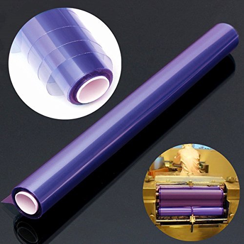
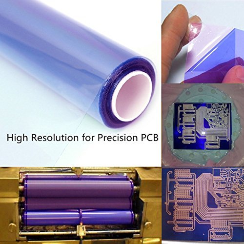
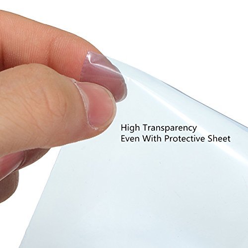
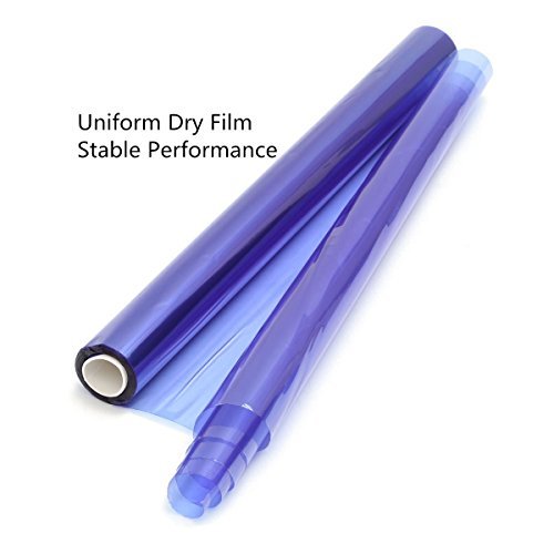
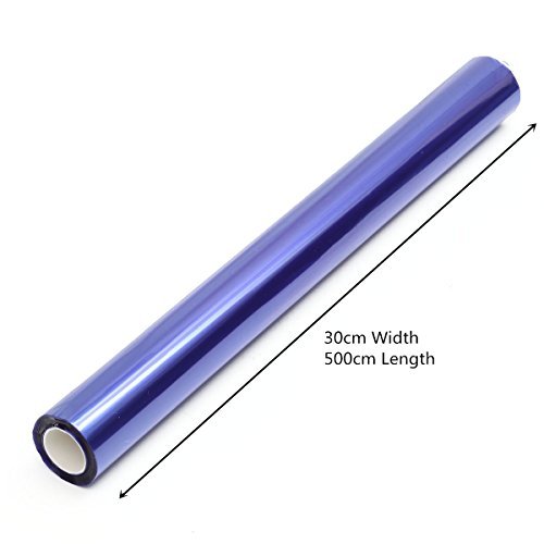
Photographic dry film is used to make PCB board, stick it on PCB to make a sensitive circuit board. Feature: Masking capacity: 0.25inch Thickness: 38±2um Size: 500cmx30cm High resolution Easy to fade and filter Good contrast before and after exposure Etching: The dry film is resistant to most of the acid etching solution, the PH value can be resistant to most alkaline etching solution between PH8.0-8.5. Cover hole: 1.5 mil dry film can fully cover a 0.25 inches thickness hole. Plating: The dry film is available in most common use of the plating bath, no wrinkles, no color.
Package Included: 1x photosensitive dry film/in a pack.
Suggestions for use 1. Foil parameters Temperature of reel : 100~120℃(210~248℉) Pasting speed: 1.0~3.0m/min (3~10feet / min) Pasting pressure: 35~50psi Plate temperature: 40 to 65℃(105 to 149℉) 2. Exposure parameters Exposure energy: 30-70mj/cm2 After exposure time: 15min If it can maintain the pH≧10.6 (dissolved about 2.0 mil-ft2/L), it can get a better quality of production. 3. Developing parameters Developer concentration: 0.8-1.2% Na2CO3•H2O Developer temperature: 28 to 32℃(82 to 89.6℉) Developing time:40~48 seconds (28℃/82.4℉)
Using Warning: 1. There will be organic solvent evaporation film, the room should maintain a good ventilation.2. Dry film must be opened in the yellow light operation. 3. Both PE and PET protective film can not be used again after open. 4.If a film after plating needs to be placed more than 24 hours, please use a black film or other shading to block light. 5.Because the non-photosensitive dry film contains acrylic monomers, may cause skin allergies, especially those who are more susceptible to allergies.
Storage: Should be placed in the temperature of 5℃–20℃(41℉-68℉), humidity 50%±10% of the environment, to reach the longest shelf life and validity.
I have tried many ways to mask PCB but so far this has produced very nice boards with fine traces
Had a Learning curve, regarding development. Now use a brush. It’s an adhesive problem. Not the same as “Dupont Ristone”.
This was my first time attempting such a project and after a bit of experimentation and practice using only standard household items, the results were fantastic. Here are some details about my approach:1. Working with the film: Simple yellow CFL “bug” light is bright enough to work with and doesn’t emit UV light which would expose the film.2. Peeling the inner film: Utility knife to scrape the corner and pick at the film enough to grab it.3. Laminating: Household iron set on “nylon” temp, held for 10-12 seconds. I was using small pieces of brass bar, so the flat section of the iron covered my lamination area completely.4. Exposure: A standard CFL bulb (spiral shape) emitted enough UV light from about 30 cm away to complete the exposure in about 8 minutes. I timed a series of test exposures to determine that 8 min. was optimal for this bulb and distance.5. Sodium Carbonate: You can make this easily. Simply heat some baking soda (i.e. sodium hydrogen carbonate, NaHCO3) in a hot pan on the stove for a few minutes. It will release water and carbon dioxide gas: 2 NaHCO3(s) + heat –> Na2CO3(s) + H2O(g) + CO2(g). Cliff Clavin would point out that now you know why baking soda causes baked items to puff up during cooking.6. Developing: I added about a tablespoon of sodium carbonate to about a liter of water and that solution dissolved the unexposed areas in about 5 minutes. I had some fairly fine detail in my design and all of the edges came out crisp.
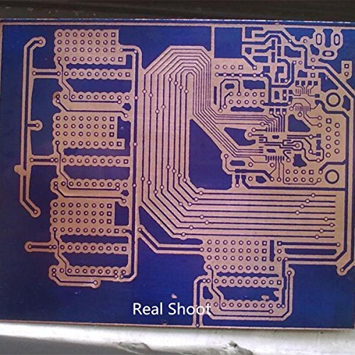
Bought the INSMA 30cm x 5M dry film and it worked great. This was my first time using photoresist and I nailed it. Roll is 5 Meters long -or- 16 Foot.This is a negative dry resist which means (Black Be Gone). Any black area on your transparency will be etched of copper. With this method you will mirror + negative print the front side, and simply negative print the rear side. If your using KiCad you can only get the negative option under “plot”, not “print”. Just change the output to PDF and Mirror/Negative options will be enabled. This also depends on the paper path in your LaserJet printer. If you use the manual drop down tray then your image will be printed on the top of the transparency and you would have to flip it over to have the toner side resting on the PCB. Whatever you see in your software -or- final PDF picture flipping the X axis and that will be the toner side down. Easy to vision.Develop: Bought some “Arm and Hammer Super Soda Ash” from my local Walmart. 100% Sodium Carbonate. Used a simple 1g/1cup of room temp water. The more dissolved in the water the better. Get yourself a meat thermometer and zero in your water faucet to around 80F or room temp. I remember this from photography class over 15 years ago. Scrub, scrub, scrub the PCB in the developer with a foam/bristle brush until all the slime is gone. Rinse and Etch. Dump your green friendly soda ash down the sink! Soda ash is typically used as an additive when washing your clothes…no problem going through your pipes.Strip: Bought some “Drano Crystals Clog Remover” from my local Home Depot after checking my local arts and crafts store Michaels. This was the only product I could find that had Sodium Hydroxide in it. There are some extra ingredients in this like aluminum flakes and some pearlite looking stuff but I had no problem at all with stripping the resist. Same formula of 1g/1cup of water. This time water temp was not checked. Scrub, scrub, scrub again until all the resist is gone. Rinse and enjoy your perfected PCB artwork!I’m drooling over the quality of my 0.250mm traces!!! Looks great. Excellent quality. Product is made in China.
Excellent
Let me just say that this stuff is awesome! Never again will I use toner transfer.This is my first attempt using photo resist and I am fully impressed.The steps I followed below.1. Peel of one side of the clear protective cover.2. Stick to copper clad board.3. Run through laminator at 110C (230F) 5-6 times.4. Place a negative of your circuit on the copper clad board and put a sheet of glass over it.5. Blast it with UV light for 5 minutes. (I purchased 395nm UV led light strips and a 12 volt adapter on eBay)6. Remove top clear protective sheet and drop it in a solution of water and sodium carbonate. 1 Gram per cup of water. (Arm & Hammer sells a giant box of this stuff at Walmart for around 5$)7. Gently brush it with a plastic bristled brush until the unexposed portion of the pcb washes off and rinse thoroughly.8. Dry and blast with UV light for another 2-3 minutes.9. Etch in ferric chloride (found on amazon)10. Rinse thoroughly.11. Drop in a container of acetone and gently brush to remove remaining film.12. Rinse and dry.Enjoy!If you wanted you could then proceed to put the solder mask on then liquid tin the pads for a truly professional looking pcb.
Just what I was looking for
Not having luck with good quality toner-transfer method so decided to try this.Despite reading the comments I can’t get anything useful from this:-Comments indicate…
I really liked this material for making boards, but it is so hard to manage without causing damage to itself.
I think im seeing the inconsistancy others have refereed to. I wear gloves, scrub my board in distilled water and 5%hcl, i give them a rinse in distilled water, rinse in acetone…
I use this stuff quite a bit. It’s great quality and easy to work with.
It worked really well for me! It was super easy to use as well!
This is not the first PCB film I’ve used, but it is, by far, the worst. It’s actually unusable because of the huge inconsistencies in thickness, meaning there are areas with so…
The photopolymer encapsulated between to two layers of acetate in the film I received was wavy and inconsistent in thickness, therefore the results were not good.
film peels easily with two pieces of tape on a corner, laminates with little problem, and gives a pretty clean exposure even when using a crude UV system (the sun and a stopwatch)…
For a first-timer like myself you have to do some experimenting with the amount of exposure, taking the protective film off both sides, etc.
comments powered by DisqusI have had a chance to make two circuit boards using this negative dry film and so far have had excellent results.